Gigabyte P55A-UD6 BIOS, Board, and Bundle
Gigabyte has been around for a long time and is a familiar brand on my test bench. Nathan reviewed the Gigabyte GA-P55-UD5 a few months back, but today we have its bigger and newer brother, the Gigabyte GA-P55A-UD6. The A signifies that the board supports USB 3.0 and SATA-III while the UD6 means it is 1 number better than the UD5. All kidding aside, the UD6 means ultra durable 6 with the number indicating how many unique features are available on the board.

This time around we have a modified Award Software BIOS. You've got all your standard menus with the important ones being the MB Intelligent Tweaker and the PC Health Status sub-menus.

The Gigabyte GA-P55A-UD6 health status isn't nearly as populated as the EVGA P55 FTW; however nearly everything is there.

I suppose the price premium of the GA-P55A-UD6 over the other boards warrants the more refined BIOS. Here you have some basic frequency and status information along with 5 convenient menus with the various settings organized by category.

The Status sub-menu provides detailed information on the assorted system frequencies and the memory timings. This is quite useful for a quick glance to see if everything is how it should be.

The frequency sub-menu gives you the ability to quickly adjust the core multiplier, QPI multiplier, base-clock frequency, PCIe frequency, and the memory divider. After digging through the BIOS of dozens of boards you start to appreciate the little things such as organization.

The advanced memory sub-menu lets you tinker with the memory sub-timings, enable an XMP profile, and tinker with the memory related voltages. Here I feel is Gigabyte's first mistake in this BIOS: individual sub-menus for each memory channel. Never once in my life have I wanted to adjust the timings between channels except for the RTL value, which can be conveniently labeled CHA and CHB. This is not a huge flaw, just a minor issue and observation.

There is nothing too special here; Gigabyte gives you enough voltage options to kill any CPU dead multiple times over. The load-line calibration can be quite helpful; I found Level 2 reduced it as much as possible and made for much more stable 24/7 overclocks.

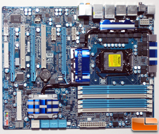
The Gigabyte P55A-UD6 has a functional layout providing easy access to all the normally used devices. The excessively large heat-piped heatsink is over the top and uncalled for but otherwise the layout is great. Those legacy IDE/FDD connectors are hiding away towards the bottom of them. Removing them could have helped declutter this packed board a bit.

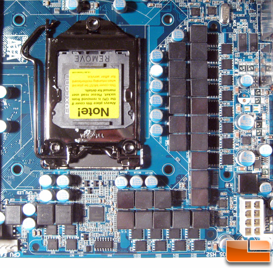
The socket is packed with components due to the "24" phase PWM. Gigabyte has switched over to the LOTES bracket after the controversy over Foxconn socket/bracket combinations melting at high current draw.

While the P55A-UD6 has 6 memory slots it is still limited to dual-channel operation and 16GB capacity due to the LGA1156 CPU. The addition of 2 additional memory slots doesn't make a lot of sense from an enthusiast point of view so I suspect this is meant to be another marketing move like the 24 phase PWM.

Tucked away between the edge of the board and the DIMM slots is a system power button. It is kind of confusing as to why this button is stuffed up here or, more importantly, why it isn't accompanied with a reset button.

This corner of the board is quite busy. The six blue SATA-II ports are provided by the P55 PCH while the two white SATA-III ports are provided by a Marvel SATA-III chip. The system reset button is sitting between the POST LED reader and the SATA-III ports. The clear CMOS button is camouflaged about an inch to the left of the POST LED reader.

Here is a clearer image of the LED POST reader, reset switch, and SATA-III ports.

The PCIe layout is typical of P55 boards with the first two PCIe x16 slots driven by the processor and the remainder of the slots driven through the P55 PCH. The second PCIe x16 slot is only electrically x8 due to the PCIe limitations of the P55 platform. Hiding at the edge of the bed is an FDD connector in quite possibly the worst possible position if you actually have to use it.

The IO options abound with this board. Most importantly are the two blue USB 3.0 connectors provided by the NEC USB 3.0 chip. 6 USB 2.0 ports are available along with two combined USB 2.0 and eSATA ports, optical and coaxial audio output, 6 audio jacks, dual gigabit Ethernet ports, and two FireWire ports. Last, but not least, is a legacy PS/2 port hanging on for dear life at the edge of the IO cluster.

Popping off the rollercoaster heatpipe solution reveals a "24" + 2 PWM feeding the core and uncore. In my opinion the ordered rows of fets and chokes are laughable and I would much rather see a 6 or 12 phase PWM. There is such thing as too much and Gigabyte has found it.

The P55 PCH is hidden away under the central heatsink on the heatpipe rollercoaster which makes you wonder what is hiding under the bottom of the rollercoaster?

On the left you have the Marvel SATA-III chip and on the right you have the iTE IDE chip.

The P55A-UD6 uses an ICS 9LPRS914EKLF PLL which is supported by setFSB and makes for very easy base clock manipulation in Windows.

The back of the P55A-UD6 is the most busy I've seen in a while. Matching the fets on the front of the board are twins on the backside, meaning each fet pair is handling less than 10 watts in a worst case scenario. Overkill?

Since the X38/P45 era Gigabyte has been slowly evolving their box-art with flashy graphics and the use of reflective coatings. I do appreciate that the board model is clearly visible along with the unique USB 3.0 support; this makes it possible to easily spot the box on the shelf so the bright colors do indeed work out well.

The P55A-UD6 bundle is quite replete with a fistful of SATA cables along with an SLI connector and an eSATA connector.

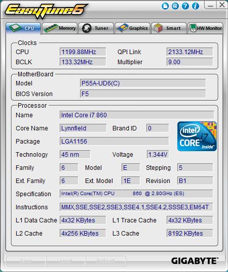
Over the last two years I have slowly watched the Gigabyte Easy Tune program evolve. The interface has become far less clunky and bizarre as in the past but it still has some room for improvement. Gigabyte should take a page out of eVGA's playbook and ink a deal with CPU-Z for an E-LEET clone.

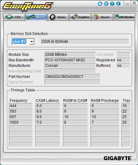
The memory tab shows you the SPD settings that are available with the currently installed memory modules.

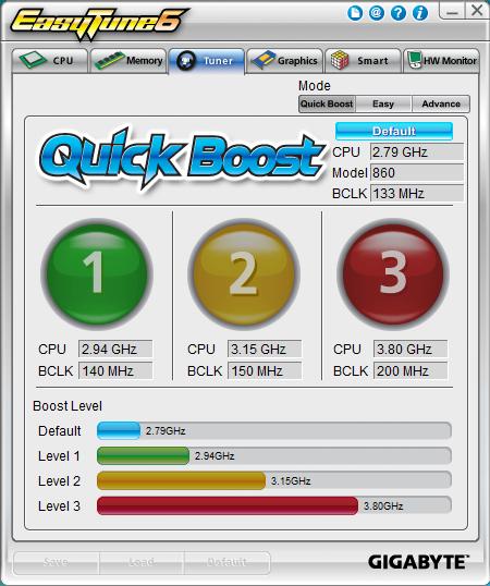
The Tuner sub-menu has two options: Quick Boost for automated overclocking and the Advanced tab for more precise overclocking. We'll be ignoring the Easy tab due to it being a cut down copy of the Advanced option. In my testing the first two options worked fine with Quick Boost but the third option for 200MHz base clock failed to POST regardless of how the stars were aligned. That all being said, I would highly suggest manually overclocking as this board is capable of much more than 200MHz base clock.

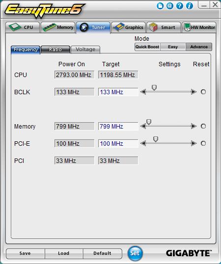
The Advance tab gives you access to lots of frequency and voltage options that can be very useful for fine-tuning your system while in the OS. I have a minor issue with the navigation layout from a usability standpoint as it requires opening ET6, clicking on the tuner tab, and then clicking on the Advance tab just to adjust the important settings. Sure, that is only 1 more click required than E-LEET but nothing gets more frustrating than spending time navigating menus, hence why I love the GA-P55A-UD6 BIOS layout over the P55 FTW BIOS layout.

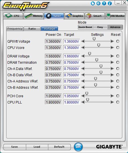
Not to get too far off track, here are the voltage options available to you. Once again, this is very useful for getting that last bit of stability out of a benchmark.


